
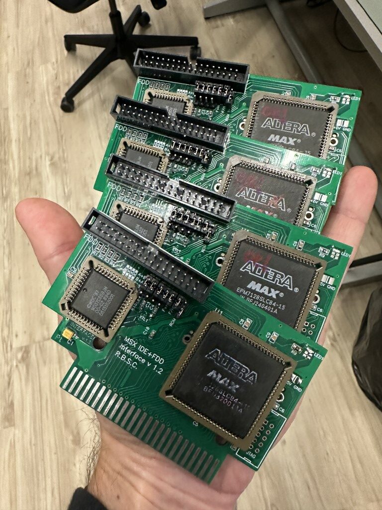
In 2015, the Russian Bear Service Crew (RBSC) introduced the FDD-IDE Multicontroller, an MSX cartridge. This controller allows users to connect up to two floppy drives and one Compact Flash card-based to any MSX computer. The cartridge features a jumper to select between the Sunrise or Nextor BIOS for disk drive operation.
When using PC floppy drives with the cartridge, the capacity is limited to 720KB. This flexible solution enables users to copy files between the Compact Flash and floppy drives and also supports the connection of GOTEK devices to the MSX.
Be aware that if you opt for the Sunrise BIOS, partitions are limited to a maximum size of 32MB. However, with the Nextor BIOS, partitions can be as large as 4GB.
Bill of Materials
The table below lists the components needed to build the cartridge, along with links to purchase each item. Please note that I do not endorse any of these sellers; the links are provided solely for your convenience.
| Reference | Value | Description | Qty | Link |
| PCB-MSX-IDE-FDD | N/A | MSX FDD-IDE Cartridge version 1.2 Printed Circuit Board | 1 | PCBWay |
| EPM7128SLC84 | PLCC84 | CMOS EEPROM-based programmable logic devices (CPLD) – 5V | 1 | AliExpress |
| SOCKET-SMD-PLCC84 | PLCC84 | SMD SMT PLCC SOCKET ADAPTER IC Block 84P PLCC84 | 1 | AliExpress |
| C3 | 15pF | 0603 15pF Ceramic Capacitor (150) | 1 | AliExpress |
| C4 | 47pF | 0603 47pF Ceramic Capacitor (470) | 1 | AliExpress |
| WD37C65BJM | PLCC44 | Floppy Disk Subsystem Controller | 1 | AliExpress |
| SOCKET-SMD-PLCC44 | PLCC44 | SMD SMT PLCC SOCKET ADAPTER IC Block 44P PLCC44 | 1 | AliExpress |
| C5, C10 | 100nF | 0603 100NF Ceramic Capacitor (104) | 2 | AliExpress |
| C2, C8, C9, C6, C7, C12 | 100nF | 0805 100NF Ceramic Capacitor (104) | 6 | AliExpress |
| C1, C11 | 10uF 16V | Tantalum Capacitor SMD Case B 16V 10uF (106C) | 2 | AliExpress |
| R1,R2,R3,R4,R5 | 200R | 0805 200 Ohm Resistor (can be 150-330R) | 5 | AliExpress |
| R6,R7,R8 | 10KR | 0805 10K Ohm Resistor | 3 | AliExpress |
| R9 | 750R | 0805 750 Ohm Resistor | 1 | AliExpress |
| R10, R15 | 1KR | 0603 1K Ohm Resistor | 2 | AliExpress |
| R11,R12,R13,R14 | 4.7KR | 0603 4.7K Ohm Resistor | 4 | AliExpress |
| 29F040B | PLCC32 | 4 Megabit (512K x 8) CMOS 5.0 Volt-only, Uniform Sector Flash Memory | 1 | AliExpress |
| SOCKET-SMD-PLCC32 | PLCC32 | SMD SMT PLCC SOCKET ADAPTER IC Block 32P PLCC32 | 1 | AliExpress |
| PH-254-S-M-40-B | 2.54 40 | 2.54mm 1 x 40 Pin Male Single Row Pin Header Strip Blue | 1 | AliExpress |
| CF-SOCKET | 50P-26MM | CF Card Socket, Card Slot 50p socket, connector, arm length 26 mm low board | 1 | AliExpress |
| LED1 | 0603-LED | 0603 LED Red | 1 | AliExpress |
| J1 | BOXED-2x17P-2.54-180 | Straight 34 PIN 2.54MM pitch MALE SOCKET idc box headers PCB CONNECTOR DOUBLE ROW | 1 | AliExpress |
| Q1 | CRY-16MHZ-HC-49S | 16M 16MHZ 20PF QUARTZ CRYSTAL RESONATOR HC-49S | 1 | AliExpress |
Building Process
The board features a mix of SMD 0805 and 0603 resistors, capacitors, and LEDs. All the ICs are in PLCC packages, which can be challenging to solder and ensure proper connections, especially if you are not accustomed to using a hot table or hot air gun.
I recommend using SMD PLCC sockets, as they are easier to solder. Additionally, given the prevalence of counterfeit/deffective chips on the market, using sockets makes it simpler to replace any faulty chips. I had to cut edges of some of the sockets to avoid having them overlapping the jumpers that are required to configure and use the cartridge.

In my experience, I purchased ten EPM7128SLC84 CPLDs, but only four were usable.
The rest of the board is straightforward to solder.
Programming the CPLD
To program the CPLD you will need a USB blaster programmer and provide 5V to power the board. The 5V can be provided by connecting the cartridge to a MSX slot of via the two contacts located on the right upper side of the CPLD.
It is highly recommended that you don’t use your MSX slot to power the board. Any errors during the building process can short the 5V power rail to ground and burn components in your MSX computer.
Instead, solder two pins to the appropriate contacts in the board and use a bench power supply to provide 5V and program the CPLD.


Follow the steps below to program the chip:
- Plug your USB blaster to your PC and connect a double male pin header to the device. You will use those pin headers to make contact to the appropriate JTAG connector on the cartridge. I opted for not soldering a boxed connector because I used sockets to host the chips and there is no space to have the JTAG connector placed on the board.
- Connect 5V and GND into your bench power supply and adjust to 5V.
- Run Quartus programmer and click Add File. Select the fdd_ide.pof file that was downloaded as part of the project package from Github.
- Connect the USB blaster programmer to the JTAG connector that is located on the side of the CPLD chip and hold with your hand to keep contact in all pins.
- Select Program/Configure and click Start. You should see success 100% progress and the success message on the upper right corner of the programmer.


Flashing the BIOS ROM
Since we are using the AM29F040B flash memory, the FDD-IDE_V21_29F040.ROM file will be used. To flash the memory chip we will use the TL866II universal programmer with the XGPRO software. Since the chip is using the PLCC32 packaging, you will also need a PLCC32 to DIP32 adapter.


You can easily find the programmer and appropriate adapter on AliExpress following the links provided below:
- TL866II
- Adapter
Below are the steps to flash the memory chip using the XGPRO and the TL866II universal programmer:
- Plug the TL866II programmer into you PC, insert the AM29F040B chip into the adapter and insert the adapter into the programmer.
- Run XGPRO and click the Select menu, choose the Search and Select IC option.
- Search for the AM29F040B chip and select the PLCC32 packaging. Click Select.

- Now click File, and then Load. Navigate to the folder where you downloaded the project files and select the FDD-IDE_V21_29F040.ROM file. Click OK.
- Now click Device and Select Program.


Usage Instructions
The cartridge features a set of jumpers for configuring the hardware and internal software. There are four 3-pin jumpers and three 2-pin jumpers. The 3-pin jumpers are used to configure the DS (drive select) signal, while the 2-pin jumpers configure the on-board devices and BIOSes.

When all 3-pin jumpers are in the upper position, a standard PC drive (with the default DS1 setting) can be connected using a standard PC floppy cable. A maximum of two drives can be connected to the cartridge: the drive connected to the middle cable connector will be B:, and the drive connected to the end of the cable will be A:.
When all 3-pin jumpers are in the lower position, a standard PC drive (with the default DS2 setting) can be connected using a standard PC floppy cable. Again, a maximum of two drives can be connected: the drive connected to the middle cable connector will be A:, and the drive connected to the end of the cable will be B:.
When the 3-pin jumpers are set for DS0 (as marked on the cartridge), a DS/DD 720KB drive with the DS0 setting can be connected using a straight floppy cable (a PC cable with a “twist” won’t work). Only one drive can be connected in this configuration.


The “F+H” jumper enables or disables the expanded slot. If the jumper is set, both the floppy controller and IDE controller are enabled. If the jumper is off, only one controller is enabled (see below).
The “F/H” jumper sets the priority for the controllers when the “F+H” jumper is installed. If the “F/H” jumper is set, the IDE controller is the first device, and the floppy controller is the second. If the “F+H” jumper is not installed, the “F/H” jumper enables only one controller—either the floppy or IDE controller. A set “F/H” jumper enables the IDE controller in this case.
The “ROM 1/2” jumper selects which IDE BIOS the cartridge will use. A set jumper enables the “Sunrise” BIOS; otherwise, the “Nextor” BIOS will be enabled.
Cartridge Case
A few months ago the RBSC team updated the GitHub repository with a case for the cartridge. I decided to customize the template I have to fit the cartridge and also went ahead and created a label for the cartridge featuring their logo. I will create a pull request on their GitHub to allow the use of those items for others with the intention to build the cartridge.
Meanwhile you can get the files here:
- Multicontroller Case Side 1 – RBSC Multicontroller (1).stl
- Multicontroller Case Side 2 – RBSC Multicontroller (2).stl


